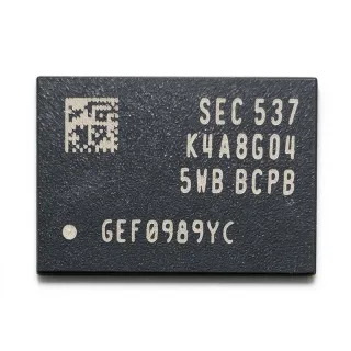
K4A8G045WB - 8Gb DDR4 SDRAM 2Gx4 2133Mbps 1.2V | Samsung
MPN: K4A8G045WB ✓ Active| Qty | Unit Price | Extended |
|---|---|---|
| 1 | $9.27 | $9.27 |
| 10 | $9.27 | $92.70 |
| 100 | $9.27 | $927.00 |
| 500 | $9.27 | $4,635.00 |
| 1,000 | $9.27 | $9,270.00 |
K4A8G045WB Overview
DDR4 SDRAM (Double Data Rate 4 Synchronous Dynamic Random Access Memory) is the fourth generation of JEDEC-defined DRAM, sitting within the memory hierarchy as a main-memory technology for servers, workstations, embedded controllers, and networking equipment. Compared with DDR3, DDR4 lowers operating voltage from 1.5 V to 1.2 V, doubles bank groups for higher bandwidth, and adds features such as posted CAS, programmable CAS latency (CWL), internal (self) calibration, on-die termination via the ODT pin, and asynchronous reset.
Key features of the K4A8G045WB include its 8 Gb B-die density, a x4 (2G x 4) organization suited to ECC-protected server and communications memory subsystems, and a maximum supply current of approximately 211.7 mA. Samsung DDR4 delivers high bandwidth with improved reliability and reduced energy consumption versus previous generations.
Technically, all control and address inputs are synchronized to a pair of externally supplied differential clocks (CK and CK#), with inputs latched at the crosspoint of the differential clock edges. The datasheet specifications apply to DLL-enabled mode of operation and represent an abstract of the full DDR4 specification; common features are covered in the separate DDR4 SDRAM Device Operation & Timing Diagram document.
Typical applications include server DIMMs and ECC memory modules, networking and telecom line cards, industrial controllers, and embedded computing platforms that require high-density, power-efficient main memory. The x4 organization makes the part especially attractive where chipkill-class ECC schemes are required.
When designing with this device, verify the exact speed grade and temperature suffix in the full ordering part number (for example K4A8G045WB-BCPB) since speed bins and temperature ranges differ between suffixes. Signal integrity on the differential clock pair and proper ODT configuration are critical at 2133 Mbps.
This page synthesizes distributor pricing, drop-in alternatives, and practical design notes not found in the manufacturer datasheet, with pricing referenced as of 2026-09-04.
Drop-in alternatives for K4A8G045WB — same package, pin-to-pin compatible. Different-package parts requiring PCB rework are excluded.
Variants in this series
Same-series models that are drop-in compatible with K4A8G045WB (same form factor and footprint) — differing in Operating Temperature, Data Rate, Memory Type, Package, Supply Voltage.
Quick Comparison Tool — Select alternative parts for side-by-side comparison:
K4A8G045WB-BCPB
✅ Drop-In✓ In Stock
$9.0234 / Unit
View Datasheet →K4A8G045WB-BCRC
✅ Drop-In✓ In Stock
$2.95 / Unit
View Datasheet →K4A8G085WB-BICH
✅ Drop-In ⚠️ Specs Unverified✓ In Stock
$4.96 / Unit
View Datasheet →K4A8G165WB-BCRC
✅ Drop-In ⚠️ Specs Unverified✓ In Stock
$12.57 / Unit
View Datasheet →K4A8G045WB Maximum Ratings & Electrical Characteristics
| Memory Type | DDR4 SDRAM (B-die) |
| Density | 8 Gb |
| Organization | 2G x 4 |
| Data Rate | 2133 Mbps |
| Supply Voltage | 1.2 V |
| Max Supply Current | 211.7 mA |
| Operating Temperature | 0 C to +85 C |
| Package | 78-ball FBGA |
| Refresh Cycles | 8192 |
| Mounting Type | Surface Mount |
| Number of Terminals | 78 |
| Clocking | Differential clock (CK / CK#) |
| On-Die Termination | Yes (ODT pin) |
| Asynchronous Reset | Yes |
| Posted CAS | Yes |
| Programmable CWL | Yes |
| Internal (Self) Calibration | Yes |
K4A8G045WB 78-ball fbga Pin Configuration Guide
Pin configuration for K4A8G045WB (78-ball fbga package). This digital IC includes GPIO, communication interfaces (UART, SPI, I2C), and power pins. Refer to the manufacturer datasheet for alternate pin functions and configuration options. Essential for embedded system design and PCB layout.

No detailed pinout data available for K4A8G045WB.
Refer to the datasheet for full pin configuration.
Typical Applications
K4A8G045WB is suitable for 6 applications: Server ECC DIMM Modules, Networking and Telecom Line Cards, Industrial Embedded Computing, Test and Measurement Instruments, Automotive-Adjacent Gateway and Telematics Development, Data Storage and SSD Controller Buffers.
Server ECC DIMM Modules
The K4A8G045WB fits server memory subsystems because its x4 organization (2G x 4) is the standard device width for advanced ECC schemes such as chipkill and single-device-data-correction, which require x4 DRAM to isolate and correct multi-bit failures within one device. Its 8Gb B-die density enables high-capacity RDIMM and LRDIMM builds, while the 1.2 V rail keeps module power within typical thermal budgets. At 2133 Mbps with DDR4 bank-group architecture, eight devices per rank deliver 64-bit channels at standard bandwidth. Design consideration: populate ranks with matched speed suffixes (-BCPB or -BCRC) and ensure SPD programming matches the controller's trained timings for reliable operation.
Recommended
Networking and Telecom Line Cards
Networking line cards, routers, and telecom switching fabric require large, deep packet buffers with deterministic latency, making 8Gb DDR4 x4 devices an excellent fit. The K4A8G045WB provides 2G x 4 depth for packet-memory pools and ECC-protected table storage, and its differential CK/CK# clocking plus on-die termination (ODT) simplify high-speed routing on dense line cards. At 2133 Mbps, a 64-bit interface sustains multi-gigabit throughput for queue management. The 0 C to +85 C range covers controlled telecom equipment environments. Design consideration: follow Samsung's fly-by topology and termination guidance, and budget the maximum 211.7 mA supply current per device in the card's power tree.
Recommended
Industrial Embedded Computing
Industrial controllers, machine-vision systems, and edge gateways use DDR4 x4 devices where memory errors are unacceptable and long product lifetimes matter. The K4A8G045WB's 8Gb density supports frame buffers and large data logging at 1.2 V, reducing overall system power in fanless enclosures. Its self-calibration and asynchronous reset features improve boot robustness in noisy industrial environments, and 8192 refresh cycles align with standard memory-controller support. Design consideration: in wide-temperature enclosures, verify junction temperature margins, since the commercial grade is rated 0 C to +85 C; for extended temperature designs, evaluate industrial-grade Samsung suffixes or derate the ambient accordingly.
Recommended
Test and Measurement Instruments
Oscilloscopes, logic analyzers, and signal generators require deep capture memory with high sustained bandwidth. The K4A8G045WB, at 8Gb per device and 2133 Mbps, allows wide parallel arrays of x4 devices to build multi-GB acquisition buffers, and the x4 organization enables per-device error scrubbing in long record acquisitions. Internal self-calibration maintains timing margins across temperature drift during extended measurement sessions, and the 1.2 V operation reduces instrument internal heating. Design consideration: equalize trace lengths across the fly-by clock network and use the ODT settings recommended in the Samsung datasheet to keep eye diagrams open at full speed.
Recommended
Automotive-Adjacent Gateway and Telematics Development
While this commercial 0 C to +85 C part is not itself AEC-Q100 qualified, the K4A8G045WB is widely used in non-safety telematics, infotainment development platforms, and industrial vehicle gateways that operate within commercial temperature limits. Its 8Gb density supports map, media, and connectivity stacks in Linux-based gateways, and 1.2 V DDR4 lowers power in always-on units. ECC via x4 organization protects long-running navigation and logging data. Design consideration: for true in-cabin or powertrain deployments, substitute an automotive-qualified DDR4 suffix and re-run signal-integrity simulation; this part should be confined to environments within its 0 C to +85 C rating.
Recommended
Data Storage and SSD Controller Buffers
Enterprise SSD controllers and storage appliances use DDR4 DRAM as mapping-table (FTL) cache and write buffers, where uncorrected bit errors corrupt metadata. The K4A8G045WB's x4 organization enables strong ECC coverage on the DRAM interface, its 8Gb density scales buffer capacity per rank, and 2133 Mbps keeps mapping lookups fast enough to sustain NVMe-class IOPS. The 1.2 V supply reduces idle power, which matters for large-buffer arrays in thermally constrained 2.5-inch and U.2 enclosures. Design consideration: implement data-retention handling for the DRAM buffer on power loss, and verify the 211.7 mA maximum per-device current when sizing the storage controller's DDR4 VRM.
Recommended
Recommended Products Summary
Engineering reference data for K4A8G045WB — comparison, design guidance, and compliance information.
Selection Guide
Comparison with Alternatives
| Parameter | This Product | K4A8G045WB-BCPB | K4A8G045WB-BCRC | K4A8G085WB | K4A8G165WB |
|---|---|---|---|---|---|
| Package | 78-ball FBGA | 78-ball FBGA - same | 78-ball FBGA - same | 78-ball FBGA family - same | 78-ball FBGA family - same |
| Brand | Samsung Electronics | Samsung Electronics | Samsung Electronics | Samsung Electronics | Samsung Electronics |
| Density | 8 Gb | 8 Gb | 8 Gb | 8 Gb | 8 Gb |
| Organization | 2G x 4 | 2G x 4 | 2G x 4 | 1G x 8 | 512M x 16 |
| Supply Voltage | 1.2 V | 1.2 V | 1.2 V | 1.2 V | 1.2 V |
Key Differentiators
- x4 organization enables advanced ECC (vs K4A8G085WB)
- Lower operating voltage than DDR3 (vs MT47H64M16NF-25E)
- B-die 8Gb density in compact FBGA (vs K4A8G165WB)
Design Notes
All control and address inputs latch at the crosspoint of the differential clocks (CK rising / CK# falling), per the Samsung datasheet. Route CK/CK# as a tightly length-matched differential pair (target intra-pair skew under 5 mils) and apply on-die termination (ODT) per the memory controller training results. At 2133 Mbps, follow DDR4 fly-by routing for address/command with per-device stubs kept minimal; run IBIS-AMI simulation with Samsung's IBIS model before tape-out to confirm eye margins.
Size the DDR4 VRM using the datasheet maximum supply current of approximately 211.7 mA per device as a starting point, then add background refresh and I/O switching current for the actual population and utilization. DDR4 also requires adequate decoupling across the VDD plane; place bulk capacitance near each device cluster plus high-frequency ceramics at every VDD ball. Ensure the regulator supports DDR4 1.2 V tolerance and startup sequencing per the controller's power-rail sequence requirements.
The Samsung datasheet explicitly notes that its timing specifications apply to DLL-enabled mode and that the document is an abstract of the full DDR4 specification - common operational features are in the separate DDR4 SDRAM Device Operation & Timing Diagram document. Do not design timing from the abstract alone; also confirm the exact suffix (-BCPB vs -BCRC) speed bin and temperature coding before BOM release, since Samsung reserves the right to change products, information, and specifications without notice.
For 78-ball FBGA DDR4, place the device close to the controller to keep fly-by clock skew within controller training range, and reference all high-speed signals to a continuous ground plane. Use controlled-impedance stackup (approximately 50 ohm single-ended per your fab's DDR4 guidance) and avoid routing DQS/DQ over plane splits. Thermal relief via the ball array is generally adequate at this power level, but verify junction temperature at worst-case refresh in high-ambient enclosures.
Compliance Information
Compliance status not stated in provided web data. Commercial temperature grade (0 C to +85 C); not AEC-Q100 qualified - Samsung AEC-Q100 grade is covered by separate automotive suffixes.