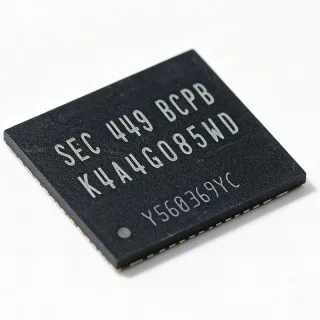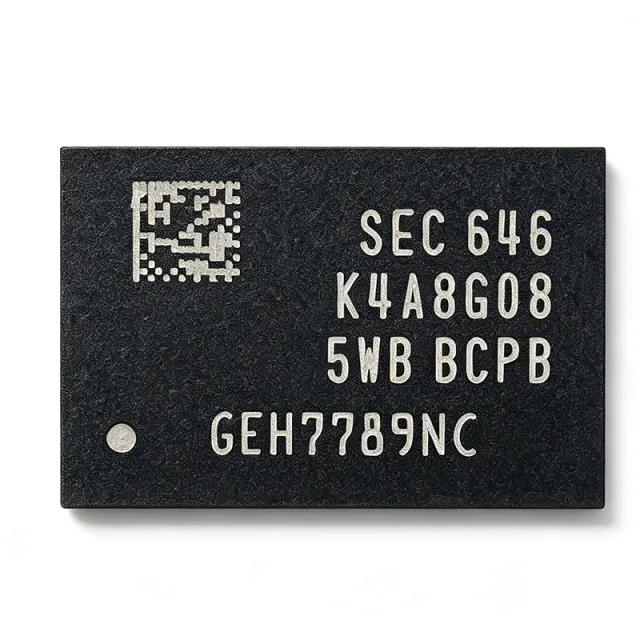
K4A8G085WB-BCPB - 8Gb DDR4 SDRAM 3200Mbps | Samsung
MPN: K4A8G085WB-BCPB ✓ Hoạt động| Số lượng | Giá đơn vị | Phụ |
|---|---|---|
| 1 | $23.625 | $23,63 |
| 10 | $17.0625 | $170,63 |
| 100 | $15.0937 | $1.509,37 |
| 500 | $14.4375 | $7.218,75 |
| 1.000 | $13.7813 | $13.781,30 |
K4A8G085WB-BCPB Tóm tắt
DDR4 SDRAM (Double Data Rate 4 Synchronous Dynamic Random Access Memory) is a volatile memory technology that transfers data on both rising and falling edges of the clock, doubling the effective data rate. Within the memory hierarchy it sits below the memory controller and above storage, serving as main system memory. DDR4 succeeded DDR3 by lowering the core supply from 1.5V to 1.2V (up to 40% power reduction), increasing bank count from 8 to 16 via bank groups, and raising densities to 8Gb and beyond.
Key features of the K4A8G085WB-BCPB include the 3200 Mbps data rate (BC speed grade), CAS Latency 22, burst length 8, and 16 banks in 4 bank groups for improved parallelism. On-die termination (ODT) and dynamic ODT improve signal integrity, while temperature-compensated self-refresh (TCSR) reduces standby power.
The device is fabricated on Samsung's advanced DRAM process (B-die generation) and supports programmable read latency (RL) and write latency (WL). It runs from a 1.2V supply (nominal) with refresh intervals of 7.8 us up to 85C operating temperature. DLL-enabled mode operation ensures precise output timing across the speed range.
Typical applications include desktop and laptop DIMMs, embedded computing boards, industrial PCs, networking equipment, and test instrumentation requiring high bandwidth in a compact footprint.
When designing in this component, match memory controller timing parameters (CL22 at 3200 Mbps), place decoupling capacitors close to the power balls, and follow the length-matched fly-by routing of DDR4 for CK/CA/DQS nets.
This page adds distributor pricing data, drop-in alternatives within the same Samsung DDR4 x8 family, and cross-brand equivalents (SK Hynix, Micron, Nanya) not found in the manufacturer datasheet alone.
Bộ thay thế dễ dàng lắp đặt cho K4A8G085WB-BCPB — cùng gói, chân-to-chân tương thích. Các bộ phận yêu cầu hàn PCB bị loại trừ.
Các biến thể trong loạt này
Các mẫu cùng loạt có thể lắp đặt dễ dàng tương thích với K4A8G085WB-BCPB (cùng hình factor và footprint) — khác nhau ở Package, Data Rate, Density, Operating Temperature, Organization.
Công cụ so sánh nhanh — Chọn các bộ phận thay thế để so sánh song song:
K4A8G085WB-BCRC
Liên hệ để biết giá
Xem tài liệu →K4A8G085WB-BITD
Liên hệ để biết giá
Xem tài liệu →K4A8G085WB-BIWE
Liên hệ để biết giá
Xem tài liệu →K4A8G085WC-BCTD
Liên hệ để biết giá
Xem tài liệu →K4A8G085WC-BIWE
Liên hệ để biết giá
Xem tài liệu →H5AN8G8NDJR
Liên hệ để biết giá
Xem tài liệu →MT40A1G8WE-075E
Liên hệ để biết giá
Xem tài liệu →K4A8G085WB-BCPB Tỷ lệ tối đa & tính chất điện
| Kiểu bộ nhớ | DDR4 SDRAM |
| Density | 8 Gbit |
| Tổ chức | 1G x 8 |
| Điện áp cung cấp | 1.2 V (nominal) |
| Tốc độ dữ liệu | 3200 Mbps (PC4-25600) |
| Speed Grade | BC |
| CAS Latency (CL) | 22 |
| Burst Length | 8 |
| Bank Architecture | 16 banks (4 bank groups) |
| Refresh Interval | 7.8 us (up to 85C) |
| Loại giao diện | SSTL-12 |
| Termination | ODT / dynamic ODT |
| Self-Refresh | Temperature-Compensated Self-Refresh (TCSR) |
| Hộp | 78-ball FBGA |
| Package Dimensions | 11 mm x 11 mm |
| Kiểu lắp đặt | Surface Mount (BGA) |
| Operating Mode | DLL enabled |
| Trạng thái RoHS | Compliant |
Cấu hình chân K4A8G085WB-BCPB
| Chân A1 | DQ0 — Data I/O bit 0 |
| Chân A2 | DQ1 — Data I/O bit 1 |
| Chân A3 | DQ2 — Data I/O bit 2 |
| Chân A7 | DQ3 — Data I/O bit 3 |
| Chân A8 | DQ4 — Data I/O bit 4 |
| Chân A9 | DQ5 — Data I/O bit 5 |
| Chân B7 | DQ6 — Data I/O bit 6 |
| Chân B8 | DQ7 — Data I/O bit 7 |
| Chân B9 | DM — Data input mask |
| Chân A4 | TDQS — Termination data strobe (tied to DQS in x8) |
| Chân B5 | TDQS# — Termination data strobe complement |
| Chân A5 | DQS — Data strobe |
| Chân B6 | DQS# — Data strobe complement |
| Chân C2 | A0 — Address input 0 |
| Chân C7 | A1 — Address input 1 |
| Chân C8 | A2 — Address input 2 |
| Chân D2 | A3 — Address input 3 |
| Chân D7 | A4 — Address input 4 |
| Chân D8 | A5 — Address input 5 |
| Chân E2 | A6 — Address input 6 |
| Chân E7 | A7 — Address input 7 |
| Chân E8 | A8 — Address input 8 |
| Chân F2 | A9 — Address input 9 |
| Chân F7 | A10 — Address input 10 / AP (auto precharge) |
| Chân F8 | A11 — Address input 11 |
| Chân G2 | A12 — Address input 12 / BC (burst chop) |
| Chân G7 | A13 — Address input 13 |
| Chân G8 | A14 — Address input 14 |
| Chân H2 | A15 — Address input 15 |
| Chân H7 | A16 — Address input 16 |
| Chân H8 | A17 — Address input 17 |
| Chân K2 | BA0 — Bank address 0 |
| Chân K7 | BA1 — Bank address 1 |
| Chân K8 | BG0 — Bank group address 0 |
| Chân L2 | BG1 — Bank group address 1 |
| Chân L7 | CK — Differential clock (positive) |
| Chân L8 | CK# — Differential clock (negative) |
| Chân M2 | CKE — Clock enable |
| Chân M7 | CS# — Chip select (active low) |
| Chân M8 | ODT — On-die termination control |
| Chân N2 | ACT# — Activation command input (active low) |
| Chân N7 | RST# — Reset (active low, pulldown) |
| Chân N8 | PAR — Command/address parity input |
| Chân P2 | ALERT# — Alert output (open drain, pulldown) |
| Chân G1 | VDDQ — DQ power supply (1.2V) |
| Chân H1 | VDDQ — DQ power supply (1.2V) |
| Chân J1 | VDDQ — DQ power supply (1.2V) |
| Chân K1 | VDDQ — DQ power supply (1.2V) |
| Chân G9 | VSSQ — DQ ground |
| Chân H9 | VSSQ — DQ ground |
| Chân J9 | VSSQ — DQ ground |
| Chân K9 | VSSQ — DQ ground |
| Chân D1 | VDD — Core power supply (1.2V) |
| Chân E1 | VDD — Core power supply (1.2V) |
| Chân F1 | VDD — Core power supply (1.2V) |
| Chân D9 | VSS — Core ground |
| Chân E9 | VSS — Core ground |
| Chân F9 | VSS — Core ground |
| Chân M1 | VDD — Core power supply (1.2V) |
| Chân N1 | VDD — Core power supply (1.2V) |
| Chân M9 | VSS — Core ground |
| Chân N9 | VSS — Core ground |
| Chân C1 | VPP — DRAM activation power supply (2.5V) |
| Chân C3 | VPP — DRAM activation power supply (2.5V) |
| Chân C9 | VPP — DRAM activation power supply (2.5V) |
| Chân B1 | VSS — Ground |
| Chân B2 | VSS — Ground |
| Chân A6 | NC — Not connected (per datasheet) |
| Chân B3 | NC — Not connected (per datasheet) |
| Chân B4 | NC — Not connected (per datasheet) |
| Chân J2 | NC — Not connected (per datasheet) |
| Chân J7 | NC — Not connected (per datasheet) |
| Chân J8 | NC — Not connected (per datasheet) |
| Chân L1 | NC — Not connected (per datasheet) |
| Chân L9 | NC — Not connected (per datasheet) |
| Chân P1 | NC — Not connected (per datasheet) |
| Chân P7 | NC — Not connected (per datasheet) |
| Chân P8 | NC — Not connected (per datasheet) |
| Chân P9 | NC — Not connected (per datasheet) |
Ứng dụng tiêu biểu
K4A8G085WB-BCPB phù hợp cho 6 Áp dụngs: Desktop and Laptop Main Memory, Embedded Computing and Industrial PCs, Networking and Communications Equipment, Server and Data Center Memory Modules, Test and Measurement Instrumentation, Medical Imaging and Diagnostic Devices.
Desktop and Laptop Main Memory
The K4A8G085WB-BCPB is a core building block for PC4-25600 UDIMM and SO-DIMM modules used in desktop and laptop computers. Its 8Gb density in a 1G x 8 organization allows eight devices to populate a 64-bit channel with ECC on x8 lanes, while the 3200 Mbps data rate at CL22 matches mainstream DDR4 memory controller support. The 1.2V rail reduces module power versus DDR3, and dynamic ODT helps maintain signal integrity across multi-rank topologies. For module designers, the 11mm x 11mm FBGA-78 footprint aligns with standard DIMM land patterns, and TCSR trims standby power in mobile sleep states, extending battery life in portable systems.
Được đề xuất
Embedded Computing and Industrial PCs
Industrial PCs, gateways, and embedded x86/ARM boards use the K4A8G085WB-BCPB soldered down for main memory, gaining 8Gb per device without SO-DIMM sockets that suffer from vibration. The 1.2V DDR4 interface reduces system heat in sealed fanless enclosures, while the 3200 Mbps grade matches common chipsets such as Intel Atom and AMD Ryzen Embedded families. Designers should place per-ball decoupling capacitors and length-match fly-by control nets. For extended-temperature deployments, consider the industrial-coded -BITD sibling, which shares the same footprint, keeping the PCB unchanged while improving the operating envelope.
Được đề xuất
Networking and Communications Equipment
Switches, routers, and network appliances rely on the K4A8G085WB-BCPB for packet buffering and deep-flow tables, where the 16-bank, 4-bank-group architecture improves random-access parallelism and effective bandwidth. The x8 organization supports ECC scrubbing essential for long-uptime infrastructure, and 3200 Mbps operation keeps memory from bottlenecking multi-gigabit data paths. The 78-ball FBGA packages densely on control-line cards. Thermal design should account for continuous full-bandwidth traffic; use air flow plus thermal vias under the package, and enable ODT per the controller's calibration routine to hold margins across temperature.
Được đề xuất
Server and Data Center Memory Modules
In RDIMM and ECC UDIMM builds, the K4A8G085WB-BCPB provides the x8 width required for single-device data correction (SDDC) on Intel and AMD server platforms. The BC-grade CL22 timing at DDR4-3200 aligns with standard server memory profiles, and the B-die silicon is well characterized for high reliability. Registered modules buffer command/address to scale to 16+ DIMMs per channel population. Designers stacking dual-rank DIMMs should verify CK/CA loading and drive-strength settings, and use the manufacturer datasheet refresh tables (7.8 us up to 85C) when configuring the memory controller's refresh rate in thermally constrained chassis.
Được đề xuất
Test and Measurement Instrumentation
Oscilloscopes, logic analyzers, and arbitrary waveform generators need large, fast capture buffers, making the K4A8G085WB-BCPB a fit with its 3200 Mbps streaming capability and 8Gb per device. Multiple devices in 64-bit or 72-bit (ECC) arrays deliver the sustained write bandwidth needed for real-time acquisition without sample loss. The 1.2V interface reduces noise coupling into sensitive analog front ends versus older 1.5V DDR3 designs. Instrument designers should implement write-leveling and read-training firmware during production calibration, since FBGA soldered-down DRAM in compact boards demands precise per-trace timing closure for full-speed operation.
Được đề xuất
Medical Imaging and Diagnostic Devices
Ultrasound, digital radiography, and lab analyzers accumulate large frame buffers that the K4A8G085WB-BCPB serves with 8Gb density and 3200 Mbps bandwidth, enabling real-time image pipelines at 1.2V power levels suited to patient-adjacent equipment. The soldered FBGA-78 package avoids connector reliability issues in mobile carts, and temperature-compensated self-refresh keeps standby draw low between scans. Designers should verify refresh timing against the datasheet operating window and use ECC-capable x8 organization to protect diagnostic data integrity. Add ground-plane shielding between DRAM and analog capture front ends to preserve low-noise imaging performance.
Được đề xuất
Tóm tắt các sản phẩm được đề xuất
Dữ liệu tham khảo kỹ thuật cho K4A8G085WB-BCPB — so sánh, hướng dẫn thiết kế và thông tin tuân thủ.
Hướng dẫn chọn lựa
So sánh với các sản phẩm thay thế
| Tham số | Sản phẩm này | K4A8G085WB-BCRC | K4A8G085WC-BCTD | H5AN8G8NDJR | MT40A1G8WE-075E |
|---|---|---|---|---|---|
| Package | 78-ball FBGA | 78-ball FBGA - same | 78-ball FBGA - same | 78-ball FBGA - same (JEDEC) | 78-ball FBGA - same (JEDEC) |
| Brand | Samsung Electronics | Samsung Electronics | Samsung Electronics | SK Hynix | Micron |
| Density | 8 Gbit | 8 Gbit | 8 Gbit | 8 Gbit | 8 Gbit |
| Organization | 1G x 8 | 1G x 8 | 1G x 8 | 1G x 8 | 1G x 8 |
| Data Rate | 3200 Mbps | 2666 Mbps (RC grade) | 2666 Mbps | 2666 Mbps (JR grade) | 1866 Mbps |
| Supply Voltage | 1.2 V | 1.2 V | 1.2 V | 1.2 V | 1.2 V |
| CAS Latency | 22 | 19 (at grade rate) | 19 | 19 | 15 |
| Bank Architecture | 16 banks / 4 bank groups | 16 banks / 4 bank groups | 16 banks / 4 bank groups | 16 banks / 4 bank groups | 16 banks / 4 bank groups |
Bảo phân biệt quan trọng
- Full DDR4-3200 (BC grade) speed support (vsK4A8G085WB-BCRC)
- High-volume B-die supply base (vsMT40A1G8WE-075E)
- ECC-ready x8 organization with TDQS (vsK4A8G165WC-BCWE)
Ghi chú thiết kế
Route DDR4 using the standard fly-by topology for CK, address, and command nets with on-die termination enabled; keep DQS/DQ length-matched within the controller's specified skew window. Provide at least one 0.1uF decoupling capacitor per VDD/VDDQ ball pair placed within 2mm of the package, plus bulk capacitance at the voltage regulator module. The 78-ball FBGA footprint is JEDEC-standard, so land patterns interchange freely across Samsung, SK Hynix, and Micron x8 DDR4 devices.
The K4A8G085WB-BCPB requires two rails: 1.2V VDD/VDDQ and 2.5V VPP for word-line activation. Size the VPP rail for low average current but be aware activation peaks; do not omit VPP decoupling, as VPP droop causes cell instability errors. Estimated: total active power at DDR4-3200 per device is typically a few hundred milliwatts, dominated by I/O switching; verify against the datasheet IDD figures for your specific traffic pattern.
Configure the memory controller to the BC speed grade timing tables (CL22 at 3200 Mbps) before bring-up; running faster grade timings on slower-coded parts causes intermittent bit errors. Perform write-leveling, read training, and DQS gate calibration at every boot and at temperature extremes. When substituting the -BCRC or -BITD siblings, re-verify SPD data and controller settings - the package is identical but speed bins and temperature coding differ.
Thông tin tuân thủ
RoHS compliance per standard Samsung DRAM product data; REACH and halogen-free status not stated in provided data.