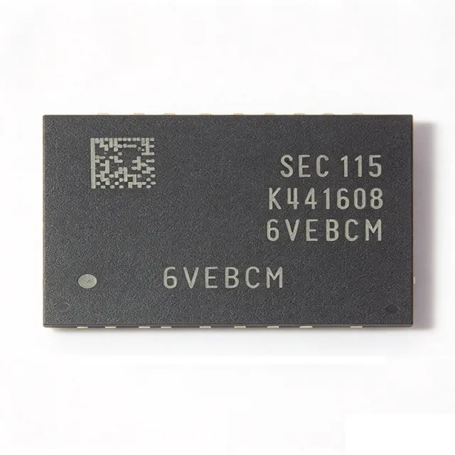
K4A8G165WC-BCTD - 8Gb DDR4 SDRAM 512Mx16 2666Mbps | Samsung
MPN: K4A8G165WC-BCTD ✓ Active| Qty | Unit Price | Extended |
|---|---|---|
| 1 | $51.42 | $51.42 |
| 10 | $48.85 | $488.50 |
| 100 | $46.12 | $4,612.00 |
| 500 | $43.55 | $21,775.00 |
| 1,000 | $41.2 | $41,200.00 |
K4A8G165WC-BCTD Overview
DDR4 SDRAM (Double Data Rate 4 Synchronous Dynamic Random-Access Memory) is the fourth generation of JEDEC-standard volatile synchronous DRAM. It transfers data on both edges of a differential clock, doubling bandwidth relative to DDR3, while lowering core voltage from 1.5V to 1.2V for improved power efficiency. In the memory hierarchy, DDR4 SDRAM sits as the main-system-memory tier within the broader DRAM family, serving servers, desktops, networking, and embedded computing platforms.
Key features of the K4A8G165WC-BCTD include auto precharge, an asynchronous reset function, CRC (Cyclic Redundancy Check) for link-level data integrity, ZQ calibration for output driver accuracy, dynamic on-chip termination (ODT) for signal quality, and a data mask function. These JEDEC-standard DDR4 features simplify board design and improve reliability at high data rates. The x16 organization allows engineers to reach large memory capacity with fewer chips and simpler address routing than x4 or x8 alternatives.
The device is built on Samsung's mature C-die DRAM process and complies with core DDR4 features such as posted CAS, programmable CAS latency (CWL), internal (self) calibration, and on-die termination via the ODT pin. All control and address inputs are synchronized to a pair of externally supplied differential clocks (CK/CK#), with inputs latched at the clock crosspoint. The operating temperature grade is 0C to +95C.
Typical applications include servers and data center memory, networking and communication equipment, industrial PCs, and embedded computing modules that require high-bandwidth, high-density DDR4 in a compact footprint.
A key design consideration: at 2666 Mbps, signal integrity is dominated by trace length matching, ODT settings, and the mandatory 240-ohm ZQ calibration resistor to ground; follow Samsung's datasheet layout guidelines and place decoupling capacitors close to the power balls.
This page synthesizes distributor pricing and stock, same-footprint drop-in alternatives across Samsung, Micron and Nanya, and practical design notes not found in the manufacturer datasheet.
Pricing as of 2026-09-04: from approximately $50.66 to $51.42 per unit at distributors such as LCSC, with several hundred units in stock.
Drop-in alternatives for K4A8G165WC-BCTD — same package, pin-to-pin compatible. Different-package parts requiring PCB rework are excluded.
Variants in this series
Same-series models that are drop-in compatible with K4A8G165WC-BCTD (same form factor and footprint) — differing in Package, Data Rate, Operating Temperature, Interface, RoHS Status.
Quick Comparison Tool — Select alternative parts for side-by-side comparison:
K4A8G165WC-BCWE
✓ In Stock
$38 / Unit
View Datasheet →K4A8G165WC-BCRC
✓ In Stock
$23 / Unit
View Datasheet →K4A8G165WB-BCTD
✓ In Stock
$37 / Unit
View Datasheet →K4A8G165WB-BIWE
✓ In Stock
$14.22 / Unit
View Datasheet →MT40A512M16LY-062E
✓ In Stock
$6.65 / Unit
View Datasheet →K4A8G165WG-BCWE
✓ In Stock
$29.5313 / Unit
View Datasheet →K4A8G165WC-BCTD Maximum Ratings & Electrical Characteristics
| Memory Type | DDR4 SDRAM |
| Density | 8 Gb |
| Organization | 512M x 16 |
| Data Rate | 2666 Mbps (DDR4-2666) |
| Supply Voltage | 1.2 V |
| Operating Voltage Range | 1.14 V to 1.26 V |
| Clock Frequency | 1.333 GHz |
| Operating Temperature | 0C to +95C |
| Package | 96FBGA (96-ball Fine-Pitch Ball Grid Array) |
| Mounting Type | Surface Mount |
| Die Revision | C-die |
| Auto Precharge | Yes |
| Asynchronous Reset | Yes |
| CRC Function | Yes |
| ZQ Calibration | Yes (240 ohm resistor to GND) |
| Dynamic On-Chip Termination (ODT) | Yes |
| Data Mask Function | Yes |
| RoHS Status | Compliant |
K4A8G165WC-BCTD 96fbga (96-ball fine-pitch ball grid array) Pin Configuration Guide
Pin configuration for K4A8G165WC-BCTD (96fbga (96-ball fine-pitch ball grid array) package). This digital IC includes GPIO, communication interfaces (UART, SPI, I2C), and power pins. Refer to the manufacturer datasheet for alternate pin functions and configuration options. Essential for embedded system design and PCB layout.

No detailed pinout data available for K4A8G165WC-BCTD.
Refer to the datasheet for full pin configuration.
Typical Applications
K4A8G165WC-BCTD is suitable for 6 applications: Server and Data Center Memory, Networking and Communication Equipment, Industrial PCs and Embedded Computing, Embedded Vision and Display Systems, Test and Measurement Instrumentation, Automotive-Adjacent Infotainment and Gateways (Non-Safety).
Server and Data Center Memory
The K4A8G165WC-BCTD fits server main-memory subsystems where 8Gb x16 density allows building large-capacity channels with fewer components. Its 2666 Mbps data rate delivers roughly 21.3 GB/s per 64-bit channel, and the 1.2V supply cuts dynamic power versus DDR3 in always-on data center operation. CRC and on-die termination support link integrity on high-utilization memory buses. Placed in fly-by topology with DDR4 register/controller training, the device sustains sustained-bandwidth workloads; the trade-off is the 0C to +95C grade, which suits climate-controlled data halls rather than unconditioned edge sites.
Recommended
Networking and Communication Equipment
Routers, switches, and 5G transport gear use the K4A8G165WC-BCTD as packet-buffer and table memory. The 512M x16 organization provides deep buffering per chip, reducing chip count on crowded line-card PCBs, while the 2666 Mbps rate sustains line-rate packet processing. Dynamic ODT and ZQ calibration maintain signal integrity across long fly-by traces typical of network backplanes, and the asynchronous reset simplifies watchdog-driven recovery logic. Designers should budget for the 0C to +95C operating range, adding convection or heatsinking for outdoor telecom cabinets operating near the upper temperature limit.
Recommended
Industrial PCs and Embedded Computing
Industrial PCs, HMIs, and embedded x86/ARM modules adopt the K4A8G165WC-BCTD for its high 8Gb density in a compact 96FBGA footprint, enabling 4 GB or more of soldered-down memory on COM Express or SMARC modules. The 1.2V operation reduces module thermal load in fanless enclosures, and CRC plus ODT preserve data integrity under EMI-heavy factory conditions. Memory is trained once at boot with standard DDR4 controller IP. The main constraint is the 0C to +95C commercial grade - cold-start environments below 0C require the wide-temperature BI-grade alternatives or local heating strategy.
Recommended
Embedded Vision and Display Systems
Video-surveillance recorders, smart displays, and embedded vision platforms use the K4A8G165WC-BCTD as frame-buffer memory. The x16 interface halves chip count for 32-bit buses versus x8 parts, which matters on cost-sensitive camera SoC boards, and 2666 Mbps sustains multi-stream 1080p60 decode plus analytics workloads. The data mask function supports efficient partial writes during video composition, and dynamic ODT handles the stub-heavy routing around camera and display connectors. At 1.2V, frame-buffer power stays low enough for passively cooled NVR enclosures with the 96FBGA's modest thermal footprint.
Recommended
Test and Measurement Instrumentation
Oscilloscopes, logic analyzers, and signal generators buffer long acquisition records in the K4A8G165WC-BCTD. Its 8Gb density allows multi-second waveform capture depths per chip, and the 2666 Mbps interface keeps real-time streaming bandwidth ahead of most front-end ADC throughputs. CRC and ZQ calibration protect long acquisition records from bit errors during deep-memory transfers, while the asynchronous reset gives instruments a deterministic memory-reset path between runs. Designers must observe the 0C to +95C ambient rating inside sealed benchtop enclosures and follow Samsung's 96FBGA layout rules for fly-by clock routing.
Recommended
Automotive-Adjacent Infotainment and Gateways (Non-Safety)
Non-safety automotive platforms such as infotainment head units, cluster SoCs, and telematics gateways use soldered-down K4A8G165WC-BCTD memory where 8Gb x16 devices let a single rank cover multimedia workloads. The 2666 Mbps rate supports simultaneous navigation rendering, media decode, and connectivity stacks, while 1.2V operation eases the thermal budget behind the dashboard. Note this BCTD part is a commercial-grade component: infotainment programs should verify that 0C to +95C coverage meets the platform's conditioning strategy, and safety-relevant domains should instead select AEC-Q100-qualified DDR4 variants from the Samsung family.
Recommended
Recommended Products Summary
Engineering reference data for K4A8G165WC-BCTD — comparison, design guidance, and compliance information.
Selection Guide
Comparison with Alternatives
| Parameter | This Product | K4A8G165WC-BCWE | K4A8G165WC-BCRC | K4A8G165WB-BCTD | MT40A512M16LY-062E | K4A8G165WB-BIWE |
|---|---|---|---|---|---|---|
| Package | 96FBGA | 96FBGA - same | 96FBGA - same | 96FBGA - same | 96FBGA - same | 96FBGA - same |
| Brand | Samsung Electronics | Samsung Electronics | Samsung Electronics | Samsung Electronics | Micron Technology | Samsung Electronics |
| Density / Organization | 8 Gb, 512M x16 | 8 Gb, 512M x16 | 8 Gb, 512M x16 | 8 Gb, 512M x16 | 8 Gb, 512M x16 | 8 Gb, 512M x16 |
| Supply Voltage | 1.2 V (1.14 V to 1.26 V) | 1.2 V (1.14 V to 1.26 V) | 1.2 V (1.14 V to 1.26 V) | 1.2 V (1.14 V to 1.26 V) | 1.2 V (1.14 V to 1.26 V) | 1.2 V (1.14 V to 1.26 V) |
| Features | Auto precharge, async reset, CRC, ZQ cal, dynamic ODT, data mask | Same JEDEC DDR4 feature set | Same JEDEC DDR4 feature set | Same JEDEC DDR4 feature set | Same JEDEC DDR4 feature set | Same JEDEC DDR4 feature set |
Key Differentiators
- Mature C-die process with proven volume production (vs K4A8G165WB-BCTD)
- Cost-optimized DDR4-2666 speed bin (vs K4A8G165WC-BCWE)
- JEDEC-standard x16 ballout enables multi-sourcing (vs MT40A512M16LY-062E)
- Full JEDEC DDR4 integrity feature set (vs Legacy DDR3 parts (e.g., K4B4G1646D))
Design Notes
For 2666 Mbps operation, route address/command lines in fly-by topology with on-die termination enabled, and length-match each DQS/DQ byte group to the datasheet skew budget. Use solid, unbroken reference planes under all DDR4 nets and keep the 96FBGA escape fanout on controlled-impedance layers. Place the 240-ohm 1% ZQ calibration resistor within a few millimeters of the ZQ ball on a short, quiet trace to ground - never share it between devices. Follow Samsung's datasheet layout section for VREF trace isolation.
The device operates at 1.2V nominal (1.14V to 1.26V). Provide separate, low-impedance VDD and VDDQ rails with bulk capacitance plus dense 0.1uF ceramic decoupling directly at the ball-side vias. Estimated: at roughly 1-2 W per chip under sustained DDR4-2666 activity, a shared 1.2V rail feeding eight chips should be sized for 8-16 W with <2% ripple. Verify VREFCA/VREFDQ generation with an accurate divider or dedicated reference and route away from switching-rail noise.
Enable dynamic ODT and perform full read/write leveling and VREFDQ training during controller initialization; at 1333 MHz clock, even small inter-pair skew causes eye closure. Simulate the fly-by stub lengths before fab - high-speed DDR4 corners on 6-layer boards typically require ODT setting optimization documented in Samsung's application notes. Keep clock (CK/CK#) differential pairs tightly coupled and length-matched to address/command groups per the controller vendor's DDR4 board design guide.
Do not substitute x8 parts (e.g., K4A8G085WB) on an x16 footprint - the ballouts differ despite identical density, and the board will not function. The BCTD grade is 0C to +95C; designs requiring cold-start below 0C must select an industrial (BI) grade variant. Also confirm the controller supports the device's speed bin and update AC timing registers when migrating to the 3200-class BCWE bin - running a slower-qualified bin at higher frequency causes intermittent errors.
Compliance Information
RoHS compliant per LCSC/JLCPCB product listings. This is a commercial/standard temperature grade part, not AEC-Q100 qualified for automotive safety applications. REACH and conflict-minerals declarations should be requested from Samsung directly.



