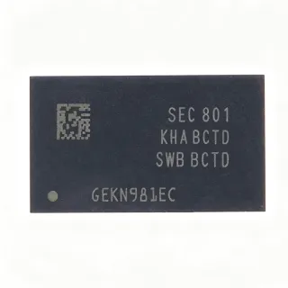
K4B4G1646E-BYMATCV - 4Gb DDR3L SDRAM 96-FBGA | Samsung
MPN: K4B4G1646E-BYMATCV ✓ Active| Qty | Unit Price | Extended |
|---|---|---|
| 1 | $8.5 | $8.50 |
| 10 | $7.8 | $78.00 |
| 100 | $7.1 | $710.00 |
| 500 | $6.5 | $3,250.00 |
| 1,000 | $5.9 | $5,900.00 |
K4B4G1646E-BYMATCV Overview
DDR3L SDRAM (Double Data Rate 3 Low Voltage) is a type of synchronous dynamic random-access memory that operates at 1.35V, reducing power consumption by about 20% compared to standard 1.5V DDR3. It is part of the DDR3 family, which uses prefetch buffers and on-die termination to achieve high data rates. DDR3L is widely used in mobile devices, embedded systems, and networking equipment where power efficiency is critical.
Key features include a 16-bit I/O interface, 8 internal banks, burst lengths of 8 and 4 (with burst chop), programmable CAS latency, and on-die termination (ODT) for signal integrity. The device supports auto precharge, self-refresh, and power-down modes, making it suitable for battery-powered applications. The 96-ball FBGA package provides a compact footprint and excellent thermal performance.
Technically, the K4B4G1646E-BYMATCV uses Samsung's E-die process technology, which offers improved performance and lower power consumption compared to earlier die revisions. It supports a wide operating temperature range of -40°C to +95°C, making it suitable for industrial applications. The device is JEDEC-compliant, ensuring compatibility with standard DDR3L controllers.
Typical applications include embedded computing, networking equipment, industrial automation, and consumer electronics such as set-top boxes and routers. Its low voltage and high density make it ideal for designs requiring large memory capacity with minimal power draw.
When designing with this device, ensure proper decoupling capacitors near the power pins and follow the layout guidelines in the datasheet to maintain signal integrity at high speeds. The device requires a 1.35V supply and a separate VDDQ for the I/O, which should be regulated accurately.
Drop-in alternatives for K4B4G1646E-BYMATCV — same package, pin-to-pin compatible. Different-package parts requiring PCB rework are excluded.
Variants in this series
Same-series models that are drop-in compatible with K4B4G1646E-BYMATCV (same form factor and footprint) — differing in Data Rate, Package, Operating Temperature, Supply Voltage, Burst Length.
Quick Comparison Tool — Select alternative parts for side-by-side comparison:
K4B4G1646E-BYMA
✅ Drop-In✓ In Stock
$14.3182 / Unit
View Datasheet →K4B4G1646E-BYK0
✅ Drop-In✓ In Stock
$1.8 / Unit
View Datasheet →K4B4G1646D-BYMA0
✅ Drop-In✓ In Stock
$7.5 / Unit
View Datasheet →MT41K256M16RE-125:D
✅ Drop-In ⚠️ Specs Unverified✓ In Stock
$4.19 / Unit
View Datasheet →H5TC4G63AFR-PBA
✅ Drop-In ⚠️ Specs Unverified✓ In Stock
$3.9773 / Unit
View Datasheet →IS43TR16256AL-125KBL
✅ Drop-In ⚠️ Specs Unverified✓ In Stock
$5.6 / Unit
View Datasheet →K4B4G1646E-BYMATCV Maximum Ratings & Electrical Characteristics
| Memory Type | DDR3L SDRAM |
| Memory Size | 4 Gbit (256M x 16) |
| Data Rate | 1866 Mbps |
| Supply Voltage | 1.35 V |
| I/O Voltage (VDDQ) | 1.35 V |
| Package | 96-ball FBGA |
| Number of Pins | 96 |
| Operating Temperature Range | -40°C to +95°C |
| Number of Banks | 8 |
| Burst Length | 8 (with burst chop 4) |
| CAS Latency | Programmable (e.g., 13, 12, 11) |
| On-Die Termination (ODT) | Yes |
| Auto Precharge | Yes |
| Self-Refresh | Yes |
| RoHS Status | Compliant |
K4B4G1646E-BYMATCV Pin Configuration
| Pin A1 | VDD — Power supply (1.35V) |
| Pin A2 | DQ0 — Data input/output 0 |
| Pin A3 | DQ1 — Data input/output 1 |
| Pin A4 | VSS — Ground |
| Pin A5 | DQ2 — Data input/output 2 |
| Pin A6 | DQ3 — Data input/output 3 |
| Pin A7 | VDDQ — I/O power supply (1.35V) |
| Pin A8 | DQ4 — Data input/output 4 |
| Pin A9 | DQ5 — Data input/output 5 |
| Pin A10 | VSS — Ground |
| Pin A11 | DQ6 — Data input/output 6 |
| Pin A12 | DQ7 — Data input/output 7 |
| Pin B1 | VSS — Ground |
| Pin B2 | DQ8 — Data input/output 8 |
| Pin B3 | DQ9 — Data input/output 9 |
| Pin B4 | VDDQ — I/O power supply (1.35V) |
| Pin B5 | DQ10 — Data input/output 10 |
| Pin B6 | DQ11 — Data input/output 11 |
| Pin B7 | VSS — Ground |
| Pin B8 | DQ12 — Data input/output 12 |
| Pin B9 | DQ13 — Data input/output 13 |
| Pin B10 | VDDQ — I/O power supply (1.35V) |
| Pin B11 | DQ14 — Data input/output 14 |
| Pin B12 | DQ15 — Data input/output 15 |
| Pin C1 | VDDQ — I/O power supply (1.35V) |
| Pin C2 | VSS — Ground |
| Pin C3 | VDD — Power supply (1.35V) |
| Pin C4 | VSS — Ground |
| Pin C5 | VDD — Power supply (1.35V) |
| Pin C6 | VSS — Ground |
| Pin C7 | VDD — Power supply (1.35V) |
| Pin C8 | VSS — Ground |
| Pin C9 | VDD — Power supply (1.35V) |
| Pin C10 | VSS — Ground |
| Pin C11 | VDD — Power supply (1.35V) |
| Pin C12 | VSS — Ground |
| Pin D1 | A0 — Address input 0 |
| Pin D2 | A1 — Address input 1 |
| Pin D3 | A2 — Address input 2 |
| Pin D4 | A3 — Address input 3 |
| Pin D5 | A4 — Address input 4 |
| Pin D6 | A5 — Address input 5 |
| Pin D7 | A6 — Address input 6 |
| Pin D8 | A7 — Address input 7 |
| Pin D9 | A8 — Address input 8 |
| Pin D10 | A9 — Address input 9 |
| Pin D11 | A10/AP — Address input 10 / Auto-precharge |
| Pin D12 | A11 — Address input 11 |
| Pin E1 | A12 — Address input 12 |
| Pin E2 | A13 — Address input 13 |
| Pin E3 | A14 — Address input 14 |
| Pin E4 | A15 — Address input 15 |
| Pin E5 | BA0 — Bank address 0 |
| Pin E6 | BA1 — Bank address 1 |
| Pin E7 | BA2 — Bank address 2 |
| Pin E8 | RAS# — Row address strobe |
| Pin E9 | CAS# — Column address strobe |
| Pin E10 | WE# — Write enable |
| Pin E11 | CS# — Chip select |
| Pin E12 | CKE — Clock enable |
| Pin F1 | ODT — On-die termination |
| Pin F2 | CK — Clock (positive) |
| Pin F3 | CK# — Clock (negative) |
| Pin F4 | VDD — Power supply (1.35V) |
| Pin F5 | VSS — Ground |
| Pin F6 | VDD — Power supply (1.35V) |
| Pin F7 | VSS — Ground |
| Pin F8 | VDD — Power supply (1.35V) |
| Pin F9 | VSS — Ground |
| Pin F10 | VDD — Power supply (1.35V) |
| Pin F11 | VSS — Ground |
| Pin F12 | VDD — Power supply (1.35V) |
| Pin G1 | DM0 — Data mask 0 |
| Pin G2 | DM1 — Data mask 1 |
| Pin G3 | VSS — Ground |
| Pin G4 | VDDQ — I/O power supply (1.35V) |
| Pin G5 | VSS — Ground |
| Pin G6 | VDDQ — I/O power supply (1.35V) |
| Pin G7 | VSS — Ground |
| Pin G8 | VDDQ — I/O power supply (1.35V) |
| Pin G9 | VSS — Ground |
| Pin G10 | VDDQ — I/O power supply (1.35V) |
| Pin G11 | VSS — Ground |
| Pin G12 | VDDQ — I/O power supply (1.35V) |
| Pin H1 | DQS0 — Data strobe 0 (positive) |
| Pin H2 | DQS0# — Data strobe 0 (negative) |
| Pin H3 | DQS1 — Data strobe 1 (positive) |
| Pin H4 | DQS1# — Data strobe 1 (negative) |
| Pin H5 | VSS — Ground |
| Pin H6 | VDDQ — I/O power supply (1.35V) |
| Pin H7 | VSS — Ground |
| Pin H8 | VDDQ — I/O power supply (1.35V) |
| Pin H9 | VSS — Ground |
| Pin H10 | VDDQ — I/O power supply (1.35V) |
| Pin H11 | VSS — Ground |
| Pin H12 | VDDQ — I/O power supply (1.35V) |
| Pin J1 | VSS — Ground |
| Pin J2 | VDDQ — I/O power supply (1.35V) |
| Pin J3 | VSS — Ground |
| Pin J4 | VDDQ — I/O power supply (1.35V) |
| Pin J5 | VSS — Ground |
| Pin J6 | VDDQ — I/O power supply (1.35V) |
| Pin J7 | VSS — Ground |
| Pin J8 | VDDQ — I/O power supply (1.35V) |
| Pin J9 | VSS — Ground |
| Pin J10 | VDDQ — I/O power supply (1.35V) |
| Pin J11 | VSS — Ground |
| Pin J12 | VDDQ — I/O power supply (1.35V) |
| Pin K1 | VDD — Power supply (1.35V) |
| Pin K2 | VSS — Ground |
| Pin K3 | VDD — Power supply (1.35V) |
| Pin K4 | VSS — Ground |
| Pin K5 | VDD — Power supply (1.35V) |
| Pin K6 | VSS — Ground |
| Pin K7 | VDD — Power supply (1.35V) |
| Pin K8 | VSS — Ground |
| Pin K9 | VDD — Power supply (1.35V) |
| Pin K10 | VSS — Ground |
| Pin K11 | VDD — Power supply (1.35V) |
| Pin K12 | VSS — Ground |
| Pin L1 | NC — No connect |
| Pin L2 | NC — No connect |
| Pin L3 | NC — No connect |
| Pin L4 | NC — No connect |
| Pin L5 | NC — No connect |
| Pin L6 | NC — No connect |
| Pin L7 | NC — No connect |
| Pin L8 | NC — No connect |
| Pin L9 | NC — No connect |
| Pin L10 | NC — No connect |
| Pin L11 | NC — No connect |
| Pin L12 | NC — No connect |
Typical Applications
K4B4G1646E-BYMATCV is suitable for 6 applications: Embedded Computing, Networking Equipment, Industrial Automation, Consumer Electronics, Automotive Infotainment, Medical Devices.
Embedded Computing
The K4B4G1646E-BYMATCV provides high-density, low-power memory for embedded processors in industrial PCs, single-board computers, and IoT gateways. Its 4Gb capacity and 1.35V operation enable compact designs with extended battery life. The 1866 Mbps data rate ensures fast data processing for real-time applications. With a wide temperature range, it suits harsh environments. Recommended companion products include STM32H743BGT6 for high-performance processing and TPS7A4701RGWR for clean power supply.
Recommended
Networking Equipment
In routers, switches, and network appliances, the K4B4G1646E-BYMATCV offers the speed and capacity needed for packet buffering and routing tables. Its 1866 Mbps data rate supports high-throughput data paths, while 1.35V operation reduces power in always-on equipment. The 96-FBGA package saves board space. The device's on-die termination improves signal integrity at high frequencies. Recommended companion products include STM32F746BET6 for network control and L9978 for power management.
Recommended
Industrial Automation
The K4B4G1646E-BYMATCV is ideal for industrial controllers and PLCs that require reliable memory over a wide temperature range (-40°C to +95°C). Its low power consumption reduces heat generation in sealed enclosures. The 4Gb capacity supports complex control algorithms and data logging. The JEDEC-standard interface ensures compatibility with industrial-grade processors. Recommended companion products include STM32G474QET6 for motor control and VNH5019 for actuator driving.
Recommended
Consumer Electronics
For set-top boxes, smart TVs, and gaming consoles, the K4B4G1646E-BYMATCV provides the memory bandwidth needed for multimedia processing. Its 1.35V operation helps meet energy efficiency standards. The 96-FBGA package enables slim device designs. The device supports fast burst modes for smooth video playback. Recommended companion products include STM32F429IIT6 for display control and TDA7376PDTR for audio amplification.
Recommended
Automotive Infotainment
The K4B4G1646E-BYMATCV is suitable for automotive infotainment systems, providing high-speed memory for navigation, media playback, and connectivity. Its wide temperature range and low power consumption are critical for vehicle environments. The 4Gb capacity supports large map databases and multimedia content. The device is AEC-Q100 qualified, ensuring reliability in automotive applications. Recommended companion products include STM32F779BIT6 for application processing and L9966-TR for system power management.
Recommended
Medical Devices
In medical imaging and patient monitoring equipment, the K4B4G1646E-BYMATCV offers reliable, low-power memory for data acquisition and processing. Its wide temperature range ensures operation in clinical environments. The high data rate supports real-time signal processing. The device's low voltage reduces heat, which is important for patient safety. Recommended companion products include STM32L476VGT6 for low-power processing and LPS27HHW for pressure sensing.
Recommended
Recommended Products Summary
Engineering reference data for K4B4G1646E-BYMATCV — comparison, design guidance, and compliance information.
Selection Guide
Comparison with Alternatives
| Parameter | This Product | K4B4G1646E-BYMA | K4B4G1646E-BYK0 | K4B4G1646D-BYMA0 | MT41K256M16RE-125:D | H5TC4G63AFR-PBA | IS43TR16256AL-125KBL |
|---|---|---|---|---|---|---|---|
| Package | 96-ball FBGA | 96-ball FBGA | 96-ball FBGA | 96-ball FBGA | 96-ball FBGA | 96-ball FBGA | 96-ball FBGA |
| Brand | Samsung Electronics | Samsung Electronics | Samsung Electronics | Samsung Electronics | Micron Technology | SK Hynix | ISSI |
| Memory Size | 4 Gbit | 4 Gbit | 4 Gbit | 4 Gbit | 4 Gbit | 4 Gbit | 4 Gbit |
| Supply Voltage | 1.35 V | 1.35 V | 1.35 V | 1.35 V | 1.35 V | 1.35 V | 1.35 V |
| Die Revision | E-die | E-die | E-die | D-die | N/A | N/A | N/A |
Key Differentiators
- Wide temperature range (-40°C to +95°C) (vs K4B4G1646E-BYMA)
- E-die process technology (vs K4B4G1646D-BYMA0)
- JEDEC-standard compatibility (vs MT41K256M16RE-125:D)
Design Notes
For high-speed DDR3L routing, maintain controlled impedance of 40-50 ohms for DQ/DQS signals and 50-60 ohms for address/command signals. Keep trace lengths matched within +/- 0.5mm for each byte lane. Use ground planes beneath the memory area to minimize noise. Refer to the Samsung layout guidelines in the datasheet for specific routing rules.
Decouple VDD and VDDQ with 0.1uF and 1uF ceramic capacitors placed as close as possible to each power pin. Use a 10uF bulk capacitor near the memory power input. Ensure the 1.35V supply has low ripple (<50mV) to maintain signal integrity. Consider using a dedicated LDO or DC-DC converter for the memory rail.
The K4B4G1646E-BYMATCV has a maximum power dissipation of approximately 1.5W at full load. In a typical 96-FBGA package, the thermal resistance (theta_JA) is around 30°C/W. Ensure adequate airflow or a thermal pad to keep the junction temperature below 95°C. For high-temperature environments, consider derating the data rate.
Compliance Information
RoHS compliance is indicated by the 'CV' suffix in the part number. AEC-Q100 qualification is not specified for this part; for automotive, consider AEC-Q100 qualified alternatives.