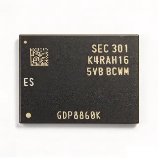
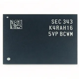
K4RAH165VB-BCWM - 16Gb DDR5 SDRAM 1.1V FBGA | Samsung
MPN: K4RAH165VB-BCWM ✓ Active| Qty | Unit Price | Extended |
|---|---|---|
| 1 | $12.22 | $12.22 |
| 10 | $11.61 | $116.10 |
| 100 | $10.99 | $1,099.00 |
| 500 | $10.44 | $5,220.00 |
| 1,000 | $9.92 | $9,920.00 |
K4RAH165VB-BCWM Overview
DDR5 SDRAM is the fifth generation of double-data-rate synchronous dynamic random-access memory, the volatile memory technology at the heart of computing systems. In the memory hierarchy, a DRAM component sits between CPU caches and non-volatile storage, providing high-bandwidth working memory. Compared with DDR4, DDR5 doubles the burst length, moves the power management IC onto the module, and lowers the per-bank granularity with independent bank group architecture, improving effective bandwidth and channel efficiency.
Key features of the K4RAH165VB-BCWM include 16Gb density in a single x16 organization, a low 1.1V core supply that reduces dynamic power, and an operating temperature range of 0C to +85C. The device integrates on-die ECC, asynchronous reset, auto self-refresh, write leveling, CRC, and ZQ calibration functions - features confirmed for the K4RAH165VB family on distributor listings.
Architecturally, the part uses a parallel memory interface with DDR5 signaling on the CA (command/address) bus, referenced to VREFCA, with DLL-enabled operation for precise timing. The x16 organization suits systems where two 16-bit devices form a 32-bit channel segment or where LPDDR-style width is preferred in embedded DDR5 designs.
Typical applications include data center memory solutions, industrial systems requiring long-term availability, high-performance computing platforms, and data-intensive consumer electronics such as tablets and mobile devices.
Designers should observe DDR5 VDDQ termination and reference voltage requirements, and verify the speed grade denoted by the BCWM suffix against the memory controller's supported JEDEC speed bins before layout sign-off.
This page synthesizes distributor pricing, drop-in family alternatives, and practical design notes not found in the manufacturer datasheet.
Drop-in alternatives for K4RAH165VB-BCWM — same package, pin-to-pin compatible. Different-package parts requiring PCB rework are excluded.
Variants in this series
Same-series models that are drop-in compatible with K4RAH165VB-BCWM (same form factor and footprint) — differing in Data Rate, Operating Temperature, Package, Interface, Density.
Quick Comparison Tool — Select alternative parts for side-by-side comparison:
K4RAH165VB-BCQK
✅ Drop-In✓ In Stock
Contact for price
View Datasheet →K4RAH086VB-BCWM
✅ Drop-In✓ In Stock
$44.5455 / Unit
View Datasheet →K4RAH086VB-BCQK
✅ Drop-In✓ In Stock
$41.0156 / Unit
View Datasheet →K4RAH086VB-BIWM
✅ Drop-In✓ In Stock
$4.85 / Unit
View Datasheet →K4RAH086VP-BCWM
✅ Drop-In✓ In Stock
Contact for price
View Datasheet →K4RAH165VB-BCWM Maximum Ratings & Electrical Characteristics
| Memory Type | DDR5 SDRAM (volatile DRAM) |
| Memory Size | 16 Gb |
| Memory Organization | 1G x 16 |
| Memory Interface | Parallel |
| Supply Voltage | 1.1 V |
| Technology | DDR5 |
| Package | FBGA-106 |
| Mounting Type | Surface Mount |
| Operating Temperature | 0C to +85C |
| Maximum Data Rate (DDR5 family) | up to 7200 Mbps |
| On-die ECC | Yes |
| Auto Self-Refresh | Yes |
| Asynchronous Reset | Yes |
| Write Leveling | Yes |
| CRC Function | Yes |
| ZQ Calibration | Yes |
| RoHS Status | Compliant |
| Packaging | Tray |
K4RAH165VB-BCWM fbga-106 Pin Configuration Guide
Pin configuration for K4RAH165VB-BCWM (fbga-106 package). This digital IC includes GPIO, communication interfaces (UART, SPI, I2C), and power pins. Refer to the manufacturer datasheet for alternate pin functions and configuration options. Essential for embedded system design and PCB layout.

No detailed pinout data available for K4RAH165VB-BCWM.
Refer to the datasheet for full pin configuration.
Typical Applications
K4RAH165VB-BCWM is suitable for 6 applications: Data Center Memory, Industrial Systems, High-Performance Computing, Mobile and Tablet Compute, Embedded DDR5 Controller Boards, Test and Measurement Instruments.
Data Center Memory
The K4RAH165VB-BCWM fits data center memory subsystems because its 16Gb density and 1G x 16 organization maximize capacity per component while the 1.1V supply cuts dynamic power, supporting Samsung's claim of ~30% better efficiency than DDR4. On-die ECC and CRC reduce error rates at high data rates, which is essential for server uptime. In a DDR5 design, two x16 devices can populate a 32-bit sub-channel segment, and the 7,200 Mbps family data rate supports high-bandwidth workloads. Designers must budget for DDR5 termination power and verify speed-grade training in the BMC/BIOS memory init code.
Recommended
Industrial Systems
Industrial controllers and edge compute platforms benefit from the K4RAH165VB-BCWM's long-term availability and 0C to +85C operating range, which covers most factory-floor and cabinet environments. The 16Gb density supports data buffering for machine vision and predictive maintenance workloads, while on-die ECC and asynchronous reset improve robustness in electrically noisy settings. Because the part runs at 1.1V, thermal design is simpler than DDR4 at equivalent bandwidth. Use the Samsung BI-grade K4RAH086VB-BIWM sibling when an industrial-grade suffix is mandated by the end customer.
Recommended
High-Performance Computing
For HPC accelerators and compute modules, the K4RAH165VB-BCWM provides 16Gb per device with DDR5 family data rates up to 7,200 Mbps, delivering the bandwidth density that bandwidth-bound scientific workloads demand. The x16 organization lets designers double density without doubling component count, and ZQ calibration plus write leveling simplify signal-integrity closure at speed on long traces. DLL-enabled mode operation guarantees the timing specifications in the Samsung datasheet. Ensure the SoC memory controller supports the BCWM speed bin and enable on-die ECC handling in firmware.
Recommended
Mobile and Tablet Compute
Samsung positions the K4RAH165VB family for mobile devices, tablets, and consumer electronics where power efficiency directly extends battery life. The 1.1V DDR5 supply and low per-bank activation granularity reduce active and standby current versus DDR4 at similar bandwidth, and the compact FBGA-106 footprint saves board area in densely packed tablets. Auto self-refresh minimizes power in suspend states. Designers should confirm the CA-bus VREFCA routing discipline and use short, length-matched DQ/DQS traces to meet DDR5 eye masks on thin flex-rigid stacks.
Recommended
Embedded DDR5 Controller Boards
Embedded designs using DDR5-capable processors, such as industrial gateway or networking SoCs, can attach the K4RAH165VB-BCWM directly as discrete DRAM. Its 1G x 16 organization pairs naturally with 32-bit DDR5 controllers using two components, and CRC plus write leveling ease bring-up on two- or four-layer stacks where signal integrity margin is limited. The asynchronous reset input allows the host to recover the DRAM without full power cycling, improving field reliability. Validate controller compatibility with the specific speed grade suffix before committing the footprint.
Recommended
Test and Measurement Instruments
High-speed oscilloscopes, logic analyzers, and signal generators require deep capture memory with sustained bandwidth; the K4RAH165VB-BCWM's 16Gb capacity and DDR5 data rates support long record lengths in acquisition engines. Its 1.1V operation reduces instrument internal power dissipation, and on-die ECC protects long-duration acquisitions from soft errors. Multiple x16 devices can be interleaved across DDR5 controllers for aggregate bandwidth. Instrument designers should implement Samsung-recommended ZQ calibration resistor placement and verify DLL lock margins across the 0C to +85C range.
Recommended
Recommended Products Summary
Engineering reference data for K4RAH165VB-BCWM — comparison, design guidance, and compliance information.
Selection Guide
Comparison with Alternatives
| Parameter | This Product | K4RAH165VB-BCQK | K4RAH086VB-BCWM | K4RAH086VB-BCQK |
|---|---|---|---|---|
| Brand | Samsung Electronics | Samsung Electronics | Samsung Electronics | Samsung Electronics |
| Package | FBGA-106 | FBGA-106 - same | FBGA (K4RAH086VB family) - verify ball map | FBGA (K4RAH086VB family) - verify ball map |
| Memory Size | 16 Gb | 16 Gb | 8 Gb | 8 Gb |
| Organization | 1G x 16 | 1G x 16 | 512M x 16 | 512M x 16 |
| Technology | DDR5 SDRAM | DDR5 SDRAM | DDR5 SDRAM | DDR5 SDRAM |
| Supply Voltage | 1.1 V | 1.1 V | 1.1 V | 1.1 V |
| Operating Temperature | 0C to +85C | 0C to +85C | 0C to +85C | 0C to +85C |
| Speed Grade (suffix) | BCWM | BCQK | BCWM | BCQK |
Key Differentiators
- Full 16Gb density in the DDR5 B-die x16 family (vs K4RAH086VB-BCWM)
- DDR5 generation power efficiency (vs K4A4G165WF-BCWE (DDR4))
- Second-sourceable within the same footprint (vs K4RAH165VB-BCQK)
Design Notes
DDR5 CA bus signaling references VREFCA, so route the CA/CS balls as a tightly length-matched group with a clean, low-impedance VREFCA decoupling network (typically 0.1 uF plus 1 uF ceramic at the DRAM side). The Samsung component datasheet defines CA eye masks relative to Vcent_CA; violations here are the most common cause of DDR5 memory-training failures. Keep CA trace stubs minimized on FBGA-106 fanout vias and simulate the eye at the target data rate before tape-out.
Although the K4RAH165VB-BCWM core runs at 1.1V, DDR5 moves the power management function toward the module/controller side, so design the 1.1V rail with sufficient transient headroom for simultaneous bank activation bursts. Estimated: at 7,200 Mbps-class operation, per-device IDD can reach several hundred milliamps during concurrent read/write bursts, so size the VRM and bulk capacitance accordingly and verify IDD figures in the Samsung datasheet IDD tables for your specific speed bin (BCWM). Do not share this rail with noisy analog supplies.
Do not substitute speed-grade suffixes without verifying the memory controller supports that JEDEC bin: BCWM and BCQK are the same die but may carry different guaranteed frequency/CAS latency, and firmware training tables are speed-bin specific. Also note the Samsung component datasheet is an abstract - the common device-operation content lives in a separate Samsung Device Operation datasheet, so obtain both documents before writing initialization code. Finally, LCSC currently shows this part out of stock as of 2026-09-04; qualify the BCQK sibling as a second source to de-risk allocation.
FBGA-106 fanout on two signal layers requires careful via planning; use via-in-pad or dog-bone fanout consistently and reserve inner layers for complete DQ/DQS/CA reference planes. DDR5 requires per-byte/per-nibble write leveling and ZQ calibration - place the ZQ calibration resistor with a short, direct trace to the ZQ ball per Samsung layout guidance. Length-match DQS to its DQ group within controller-specified skew (typically tighter than DDR4), and keep all DDR5 signals referenced to unbroken ground planes for the full trace length.
Compliance Information
RoHS compliant per JLCPCB part listing (FBGA-106 DDR SDRAM ROHS). Lead-free per standard Samsung DRAM production. REACH, halogen-free, and conflict-minerals declarations not stated in provided data - consult Samsung official compliance documentation.