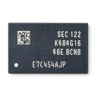
K4A4G165WD-BCTD - 4Gb DDR4 SDRAM x16 2666Mbps | Samsung
MPN: K4A4G165WD-BCTD ✓ Active| Qty | Unit Price | Extended |
|---|---|---|
| 1 | $22.47 | $22.47 |
| 10 | $21.5 | $215.00 |
| 100 | $20.75 | $2,075.00 |
| 500 | $19.9 | $9,950.00 |
| 1,000 | $19 | $19,000.00 |
K4A4G165WD-BCTD Overview
DDR4 SDRAM (Double Data Rate 4 Synchronous Dynamic Random Access Memory) is the fourth generation of the JEDEC-standardized DDR DRAM family. Within the memory hierarchy, DRAM sits as main system memory between CPU caches (SRAM) and non-volatile storage (NAND flash), and DDR4 itself evolved from DDR3 by lowering core voltage from 1.5V to 1.2V, doubling bank groups, and introducing features such as Bank Group Architecture, DBI (Data Bus Inversion), CRC, CA parity, and VPP (2.5V wordline pump supply).
Key features of the K4A4G165WD family include a 4 Gb D-die core, x16 data width with data mask (DM) and DQS strobes per byte lane, auto precharge, asynchronous reset (RESET_n), ZQ calibration (ZQ ball with external precision resistor), dynamic on-chip termination (ODT), and CRC read/write integrity checking per the Samsung DDR4 datasheet. The -BCTD speed grade supports 2666 Mbps operation at the commercial temperature range of 0C to +85C.
Architecturally, the device uses Samsung's advanced D-die process with a bank-grouped core (four bank groups, four banks per group), enabling higher effective bandwidth by allowing back-to-back accesses to different bank groups. The 1.2V VDD rail plus a separate 2.5V VPP rail reduces both dynamic and standby power versus DDR3 alternatives, and dynamic ODT optimizes signal integrity on the fly for fly-by-routed address/command buses.
Typical applications include embedded CPU and SoC main memory (NXP, TI Sitara, Rockchip class processors), industrial gateways and edge controllers, networking equipment line-card memory, and consumer electronics requiring 4 Gb x16 footprints.
A key design consideration: x16 DDR4 devices use a shared 96-ball FBGA footprint only with other x16 parts; x8 DDR4 devices are NOT pin-compatible on the same land pattern, and speed grades must be matched to the memory controller's supported DDR4 frequency training limits.
This page synthesizes verified distributor pricing, drop-in alternatives across Samsung die revisions and Micron equivalents, and practical DDR4 design notes not found in the manufacturer datasheet.
Drop-in alternatives for K4A4G165WD-BCTD — same package, pin-to-pin compatible. Different-package parts requiring PCB rework are excluded.
Variants in this series
Same-series models that are drop-in compatible with K4A4G165WD-BCTD (same form factor and footprint) — differing in Package, RoHS Status, Interface, Operating Temperature, Data Rate.
Quick Comparison Tool — Select alternative parts for side-by-side comparison:
K4A4G165WF-BCTD
✅ Drop-In✓ In Stock
$8.2031 / Unit
View Datasheet →K4A4G165WE-BCTD
✅ Drop-In✓ In Stock
$11.38 / Unit
View Datasheet →K4A4G165WD-BCRC
✅ Drop-In✓ In Stock
$5.1 / Unit
View Datasheet →K4A4G165WD-BCPB
✅ Drop-In✓ In Stock
$3.1 / Unit
View Datasheet →MT40A256M16GE-075E:B
✅ Drop-In✓ In Stock
$3.95 / Unit
View Datasheet →K4A4G165WD-BCTD Maximum Ratings & Electrical Characteristics
| Memory Type | DDR4 SDRAM |
| Density | 4 Gbit |
| Organization | 256M x 16 |
| Data Rate | 2666 Mbps/pin (-BCTD speed grade) |
| Supply Voltage (VDD) | 1.2 V |
| Core Supply (VPP) | 2.5 V |
| Interface | SSTL-12 |
| Data Mask | Yes (DM per byte lane) |
| Bank Architecture | 16 banks / 4 bank groups |
| Package | 96-ball FBGA |
| Mounting Type | Surface Mount (BGA) |
| Operating Temperature | 0C to +85C (commercial) |
| On-Die Termination | Dynamic ODT |
| ZQ Calibration | Yes (external RZQ resistor) |
| CRC / CA Parity | CRC read/write support |
| Reset | Asynchronous reset (RESET_n) |
K4A4G165WD-BCTD 96-ball fbga Pin Configuration Guide
Pin configuration for K4A4G165WD-BCTD (96-ball fbga package). This digital IC includes GPIO, communication interfaces (UART, SPI, I2C), and power pins. Refer to the manufacturer datasheet for alternate pin functions and configuration options. Essential for embedded system design and PCB layout.

No detailed pinout data available for K4A4G165WD-BCTD.
Refer to the datasheet for full pin configuration.
Typical Applications
K4A4G165WD-BCTD is suitable for 6 applications: Embedded SoC Main Memory, Industrial Gateways and Edge Controllers, Networking Equipment Buffer Memory, Consumer Electronics and Smart Home Hubs, Medical Diagnostic and Monitoring Devices, Test and Measurement Instrumentation.
Embedded SoC Main Memory
The K4A4G165WD-BCTD serves as single-chip main memory for embedded Linux SoCs with a 16-bit DDR4 controller (NXP i.MX8M, TI Sitara AM64x, Rockchip class). Its 4Gb x16 organization fills an entire 16-bit channel with one device, delivering up to 4.26 GB/s peak bandwidth at DDR4-2666 while keeping the power tree simple: one 1.2 V VDD rail and one 2.5 V VPP rail, both commonly available from standard PMICs. The x16 width minimizes PCB layer count because address/command fly-by routing to a single device avoids multi-drop stubs. Designers should size the VTT termination rail and place the 240-ohm RZQ resistor close to the ZQ ball; memory training at boot validates the 2666 Mbps interface timing against the SoC controller table.
Recommended
Industrial Gateways and Edge Controllers
Industrial edge gateways need reliable 4 Gb-class memory to buffer protocol translation, local caching, and containerized workloads. The K4A4G165WD-BCTD provides 512 MB per device at 2666 Mbps with auto precharge and asynchronous reset support, simplifying power-fail recovery sequencing in gateways that brown-out frequently. Its 0C to +85C commercial rating suits indoor cabinet deployments; for -40C outdoor designs, the -BCRC industrial variant should be evaluated instead. The 1.2 V VDD consumes roughly 25 percent less power than equivalent DDR3 solutions, reducing thermal load in sealed enclosures. Dynamic ODT and CRC help maintain signal integrity in electrically noisy factory-floor environments where long bus traces and switching transients degrade DDR margins.
Recommended
Networking Equipment Buffer Memory
Line-card packet buffering and control-plane memory in routers and switches benefit from the K4A4G165WD-BCTD's DDR4-2666 bandwidth and CRC-checked data path, which detects transmission errors on read bursts - a meaningful reliability feature when forwarding tables and queues live in DRAM. The 256M x16 organization maps naturally to 16-bit or 32-bit (two-device) control-plane subsystems on NXP Layerscape and Marvell class SoCs. Fly-by address/command routing with dynamic ODT sustains signal integrity at 2666 Mbps across the multi-load topologies typical of networking boards. Designers should budget the 2.5 V VPP rail from a dedicated LDO or PMIC output and follow Samsung's ODT settings in the mode register programming tables of the datasheet.
Recommended
Consumer Electronics and Smart Home Hubs
Smart home hubs, IPTV set-top boxes, and voice-assistant controllers use one K4A4G165WD-BCTD as affordable 512 MB system memory at DDR4-2666. Cost sensitivity in this market favors the commercial 0C to +85C grade and single-chip x16 footprint, which shortens the PCB and reduces assembly cost versus four x8 devices. The 1.2 V operation supports low idle power for always-on voice devices, and the asynchronous RESET_n ball allows the host SoC to hard-reset DRAM state during firmware recovery without power cycling. Because consumer BOMs rotate die revisions frequently, the footprint-compatible K4A4G165WF-BCTD and K4A4G165WE-BCTD siblings let purchasing substitute second sources within the same Samsung family without layout changes.
Recommended
Medical Diagnostic and Monitoring Devices
Point-of-care analyzers and patient monitors need moderate-density DRAM for waveform buffering and image processing pipelines. The K4A4G165WD-BCTD's CRC-enabled DDR4 interface adds a data-integrity layer important for diagnostic record accuracy, while its 512 MB capacity handles FFT buffers and display frame stores. The 1.2 V core rail keeps total board power low, easing thermal design in fanless wall-mounted enclosures that must stay quiet. Medical designs typically lock a single die revision through regulatory review; the family's footprint-compatible siblings (WF, WE die) provide a documented second source for manufacturing continuity once validated. Memory training parameters from the SoC vendor should be re-validated on every board spin to preserve 2666 Mbps timing margins.
Recommended
Test and Measurement Instrumentation
Bench instruments, logic analyzers, and data-acquisition systems stream high-rate ADC data into DDR4 capture buffers. The K4A4G165WD-BCTD's 4.26 GB/s peak bandwidth at 2666 Mbps sustains multi-channel capture at 16-bit widths, and its ZQ-calibrated output impedance keeps DQ drive strength consistent across temperature drift during long acquisitions. A single 4Gb device gives 512 MB of capture depth; dual-device 32-bit configurations double both depth and bandwidth for high-end scopes. Instrument designers should implement the full power-up sequence from the Samsung datasheet (RESET_n assertion, CKE control, MRW register programming) and verify the -BCTD CAS latency (CL19 class at 2666) matches the controller's mode register table before scheduling production firmware.
Recommended
Recommended Products Summary
Engineering reference data for K4A4G165WD-BCTD — comparison, design guidance, and compliance information.
Selection Guide
Comparison with Alternatives
| Parameter | This Product | K4A4G165WF-BCTD | K4A4G165WE-BCTD | K4A4G165WD-BCRC | K4A4G165WD-BCPB | MT40A256M16GE-075E:B |
|---|---|---|---|---|---|---|
| Package | 96-ball FBGA | 96-ball FBGA - same | 96-ball FBGA - same | 96-ball FBGA - same | 96-ball FBGA - same | 96-ball FBGA - same |
| Brand | Samsung Electronics | Samsung Electronics | Samsung Electronics | Samsung Electronics | Samsung Electronics | Micron Technology |
| Density / Organization | 4 Gb / 256M x 16 | 4 Gb / 256M x 16 | 4 Gb / 256M x 16 | 4 Gb / 256M x 16 | 4 Gb / 256M x 16 | 4 Gb / 256M x 16 |
| Supply Voltage | 1.2 V VDD / 2.5 V VPP | 1.2 V / 2.5 V | 1.2 V / 2.5 V | 1.2 V / 2.5 V | 1.2 V / 2.5 V | 1.2 V / 2.5 V |
| Die Revision | D-die (WD) | F-die | E-die | D-die | D-die | Micron G-die |
Key Differentiators
- Fastest standard -BCTD speed grade (vs K4A4G165WD-BCRC)
- Single-chip 512 MB x16 memory (vs K4A4G085WD-BCTD)
- Lower cost than newer F-die sibling (vs K4A4G165WF-BCTD)
Design Notes
The K4A4G165WD-BCTD requires two supply rails: 1.2 V VDD/SSTL-12 interface and 2.5 V VPP wordline pump. Never interchange them - 2.5 V on VDD destroys the die. Estimated power check: at DDR4-2666 with ~50 percent read activity, a 4Gb x16 device typically draws a few hundred milliamps on VDD; size the 1.2 V rail with at least 22 uF of bulk plus per-ball 0.1 uF decoupling on VDD, VDDQ, and VPP. Power up VPP and VDD before or together with VDDQ per the Samsung DDR4 datasheet power-up sequence, and hold RESET_n low through ramp.
At 2666 Mbps, route DQ/DQS/DM as length-matched groups with DQS strobes as differential pairs; keep intra-pair skew tight and total flight-time skew within the controller training window. Use fly-by routing for address/command/CKE/ODT with dynamic ODT enabled and VTT termination (0.6 V, capable of sinking/sourcing peak currents during bus turnaround). The ZQ ball requires a 240-ohm 1 percent resistor to VSS placed within a few millimeters. Simulate ODT settings (Rtt_Nom/Rtt_WR) against your stackup before locking the PCB.
x16 and x8 DDR4 devices share the 96-ball FBGA package size but have DIFFERENT ballouts - a K4A4G085WD x8 part cannot replace this x16 device on the same footprint. Also confirm die revision compatibility with your SoC memory training table before swapping WD/WF/WE die letters; boot failures at DDR4-2666 are the most common substitution symptom. Finally, verify the speed code: -BCRC parts are slower (2133-class) and will not meet DDR4-2666 timing requirements.
Place the DRAM within a few centimeters of the SoC for DDR4-2666 operation on two- to four-layer boards. Maintain a solid, unbroken reference plane under all DDR4 nets; do not route DQS pairs across plane splits. Use via-in-pad or short stubs on BGA escape, and reserve copper pour area under the 96-ball FBGA (est. thermal enhancement) since JEDEC-standard FBGA theta-JA depends heavily on board copper. Add test points on DQS0/DQS1 pairs for signal integrity bring-up and margin testing.
Compliance Information
Fetched distributor listings (LCSC, Octopart) do not display explicit RoHS/REACH compliance fields for this exact MPN. Samsung current-production DDR4 is generally RoHS-compliant; obtain the official certificate from Samsung before design-in. Not an automotive-qualified part designation.