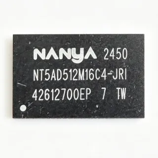
NT5CB256M16CP-DI - 4Gb DDR3L SDRAM 256Mx16 | Nanya
MPN: NT5CB256M16CP-DI ✓ Active| Qty | Unit Price | Extended |
|---|---|---|
| 1 | $8.5 | $8.50 |
| 10 | $7.8 | $78.00 |
| 100 | $7.2 | $720.00 |
| 500 | $6.8 | $3,400.00 |
| 1,000 | $6.5 | $6,500.00 |
NT5CB256M16CP-DI Overview
DDR3L SDRAM is a type of dynamic random-access memory that operates at a lower voltage (1.35V) compared to standard DDR3 (1.5V), reducing power consumption by about 20% while maintaining similar performance. It is part of the DDR3 memory family, which uses double data rate architecture to transfer data on both edges of the clock. DDR3L is widely used in mobile, embedded, and industrial applications where power efficiency is critical.
Key features include a 256Mx16 organization (4Gb density), 1.35V supply voltage, 96-ball TFBGA package, and support for data rates up to 1600 Mbps/pin. The device has a programmable CAS latency of 5-11, write latency of 5-9, and additive latency of 0-13. It also features 8 internal banks, differential clock inputs, and on-die termination. The operating temperature range is -40°C to +95°C (industrial) and -40°C to +105°C (automotive).
The NT5CB256M16CP-DI uses a 70nm process technology, enabling high density and low power consumption. It incorporates DLL (delay-locked loop) for precise timing, and supports self-refresh and partial array self-refresh for power saving. The device is RoHS compliant and lead-free.
Typical applications include embedded systems, networking equipment, industrial automation, automotive infotainment, and solid-state drives. Its low voltage and wide temperature range make it suitable for harsh environments.
When designing with this memory, ensure proper decoupling capacitors near the power pins and follow the layout guidelines in the datasheet to minimize signal integrity issues. The device requires a stable 1.35V supply and reference voltage (VREF) for optimal operation.
Drop-in alternatives for NT5CB256M16CP-DI — same package, pin-to-pin compatible. Different-package parts requiring PCB rework are excluded.
Variants in this series
Same-series models that are drop-in compatible with NT5CB256M16CP-DI (same form factor and footprint) — differing in Package, Data Rate, Supply Voltage, Operating Temperature, Burst Length.
Quick Comparison Tool — Select alternative parts for side-by-side comparison:
NT5CB256M16DP-DI
✅ Drop-In📋 Reference alternative (not in catalog)
NT5CB256M16CP-DII
✅ Drop-In✓ In Stock
$5.5682 / Unit
View Datasheet →MT41K256M16HA-125
✅ Drop-In ⚠️ Specs Unverified✓ In Stock
$6.3636 / Unit
View Datasheet →K4B4G1646E-BYMA
✅ Drop-In ⚠️ Specs Unverified✓ In Stock
$14.3182 / Unit
View Datasheet →IS43TR16512B-125K
✅ Drop-In ⚠️ Specs Unverified📋 Reference alternative (not in catalog)
NT5CB256M16CP-DI Maximum Ratings & Electrical Characteristics
| Memory Type | DDR3L SDRAM |
| Organization | 256M x 16 |
| Density | 4 Gb |
| Supply Voltage | 1.35 V (DDR3L) |
| Data Rate | 1600 Mbps/pin (max) |
| Package | TFBGA-96 |
| Number of Banks | 8 |
| CAS Latency (CL) | 5, 6, 7, 8, 9, 10, 11 |
| Write Latency (CWL) | 5, 6, 7, 8, 9 |
| Additive Latency | 0-13 |
| Operating Temperature Range | -40°C to +95°C (industrial), -40°C to +105°C (automotive) |
| RoHS | Compliant |
| Lead-Free | Yes |
| Differential Clock Input | Yes (CK, CK#) |
| On-Die Termination (ODT) | Yes |
NT5CB256M16CP-DI Pin Configuration
| Pin A1 | VDD — Power supply (1.35V) |
| Pin A2 | DQ0 — Data input/output 0 |
| Pin A3 | DQ1 — Data input/output 1 |
| Pin A4 | VSS — Ground |
| Pin A5 | DQ2 — Data input/output 2 |
| Pin A6 | DQ3 — Data input/output 3 |
| Pin A7 | VDD — Power supply (1.35V) |
| Pin A8 | DQ4 — Data input/output 4 |
| Pin A9 | DQ5 — Data input/output 5 |
| Pin A10 | VSS — Ground |
| Pin A11 | DQ6 — Data input/output 6 |
| Pin A12 | DQ7 — Data input/output 7 |
| Pin B1 | VSS — Ground |
| Pin B2 | DQ8 — Data input/output 8 |
| Pin B3 | DQ9 — Data input/output 9 |
| Pin B4 | VDD — Power supply (1.35V) |
| Pin B5 | DQ10 — Data input/output 10 |
| Pin B6 | DQ11 — Data input/output 11 |
| Pin B7 | VSS — Ground |
| Pin B8 | DQ12 — Data input/output 12 |
| Pin B9 | DQ13 — Data input/output 13 |
| Pin B10 | VDD — Power supply (1.35V) |
| Pin B11 | DQ14 — Data input/output 14 |
| Pin B12 | DQ15 — Data input/output 15 |
| Pin C1 | VDD — Power supply (1.35V) |
| Pin C2 | VSS — Ground |
| Pin C3 | VDD — Power supply (1.35V) |
| Pin C4 | VSS — Ground |
| Pin C5 | VDD — Power supply (1.35V) |
| Pin C6 | VSS — Ground |
| Pin C7 | VDD — Power supply (1.35V) |
| Pin C8 | VSS — Ground |
| Pin C9 | VDD — Power supply (1.35V) |
| Pin C10 | VSS — Ground |
| Pin C11 | VDD — Power supply (1.35V) |
| Pin C12 | VSS — Ground |
| Pin D1 | VSS — Ground |
| Pin D2 | VDD — Power supply (1.35V) |
| Pin D3 | VSS — Ground |
| Pin D4 | VDD — Power supply (1.35V) |
| Pin D5 | VSS — Ground |
| Pin D6 | VDD — Power supply (1.35V) |
| Pin D7 | VSS — Ground |
| Pin D8 | VDD — Power supply (1.35V) |
| Pin D9 | VSS — Ground |
| Pin D10 | VDD — Power supply (1.35V) |
| Pin D11 | VSS — Ground |
| Pin D12 | VDD — Power supply (1.35V) |
| Pin E1 | VDD — Power supply (1.35V) |
| Pin E2 | VSS — Ground |
| Pin E3 | VDD — Power supply (1.35V) |
| Pin E4 | VSS — Ground |
| Pin E5 | VDD — Power supply (1.35V) |
| Pin E6 | VSS — Ground |
| Pin E7 | VDD — Power supply (1.35V) |
| Pin E8 | VSS — Ground |
| Pin E9 | VDD — Power supply (1.35V) |
| Pin E10 | VSS — Ground |
| Pin E11 | VDD — Power supply (1.35V) |
| Pin E12 | VSS — Ground |
| Pin F1 | VSS — Ground |
| Pin F2 | VDD — Power supply (1.35V) |
| Pin F3 | VSS — Ground |
| Pin F4 | VDD — Power supply (1.35V) |
| Pin F5 | VSS — Ground |
| Pin F6 | VDD — Power supply (1.35V) |
| Pin F7 | VSS — Ground |
| Pin F8 | VDD — Power supply (1.35V) |
| Pin F9 | VSS — Ground |
| Pin F10 | VDD — Power supply (1.35V) |
| Pin F11 | VSS — Ground |
| Pin F12 | VDD — Power supply (1.35V) |
| Pin G1 | VDD — Power supply (1.35V) |
| Pin G2 | VSS — Ground |
| Pin G3 | VDD — Power supply (1.35V) |
| Pin G4 | VSS — Ground |
| Pin G5 | VDD — Power supply (1.35V) |
| Pin G6 | VSS — Ground |
| Pin G7 | VDD — Power supply (1.35V) |
| Pin G8 | VSS — Ground |
| Pin G9 | VDD — Power supply (1.35V) |
| Pin G10 | VSS — Ground |
| Pin G11 | VDD — Power supply (1.35V) |
| Pin G12 | VSS — Ground |
| Pin H1 | VSS — Ground |
| Pin H2 | VDD — Power supply (1.35V) |
| Pin H3 | VSS — Ground |
| Pin H4 | VDD — Power supply (1.35V) |
| Pin H5 | VSS — Ground |
| Pin H6 | VDD — Power supply (1.35V) |
| Pin H7 | VSS — Ground |
| Pin H8 | VDD — Power supply (1.35V) |
| Pin H9 | VSS — Ground |
| Pin H10 | VDD — Power supply (1.35V) |
| Pin H11 | VSS — Ground |
| Pin H12 | VDD — Power supply (1.35V) |
| Pin J1 | VDD — Power supply (1.35V) |
| Pin J2 | VSS — Ground |
| Pin J3 | VDD — Power supply (1.35V) |
| Pin J4 | VSS — Ground |
| Pin J5 | VDD — Power supply (1.35V) |
| Pin J6 | VSS — Ground |
| Pin J7 | VDD — Power supply (1.35V) |
| Pin J8 | VSS — Ground |
| Pin J9 | VDD — Power supply (1.35V) |
| Pin J10 | VSS — Ground |
| Pin J11 | VDD — Power supply (1.35V) |
| Pin J12 | VSS — Ground |
| Pin K1 | VSS — Ground |
| Pin K2 | VDD — Power supply (1.35V) |
| Pin K3 | VSS — Ground |
| Pin K4 | VDD — Power supply (1.35V) |
| Pin K5 | VSS — Ground |
| Pin K6 | VDD — Power supply (1.35V) |
| Pin K7 | VSS — Ground |
| Pin K8 | VDD — Power supply (1.35V) |
| Pin K9 | VSS — Ground |
| Pin K10 | VDD — Power supply (1.35V) |
| Pin K11 | VSS — Ground |
| Pin K12 | VDD — Power supply (1.35V) |
| Pin L1 | VDD — Power supply (1.35V) |
| Pin L2 | VSS — Ground |
| Pin L3 | VDD — Power supply (1.35V) |
| Pin L4 | VSS — Ground |
| Pin L5 | VDD — Power supply (1.35V) |
| Pin L6 | VSS — Ground |
| Pin L7 | VDD — Power supply (1.35V) |
| Pin L8 | VSS — Ground |
| Pin L9 | VDD — Power supply (1.35V) |
| Pin L10 | VSS — Ground |
| Pin L11 | VDD — Power supply (1.35V) |
| Pin L12 | VSS — Ground |
| Pin M1 | VSS — Ground |
| Pin M2 | VDD — Power supply (1.35V) |
| Pin M3 | VSS — Ground |
| Pin M4 | VDD — Power supply (1.35V) |
| Pin M5 | VSS — Ground |
| Pin M6 | VDD — Power supply (1.35V) |
| Pin M7 | VSS — Ground |
| Pin M8 | VDD — Power supply (1.35V) |
| Pin M9 | VSS — Ground |
| Pin M10 | VDD — Power supply (1.35V) |
| Pin M11 | VSS — Ground |
| Pin M12 | VDD — Power supply (1.35V) |
| Pin N1 | VDD — Power supply (1.35V) |
| Pin N2 | VSS — Ground |
| Pin N3 | VDD — Power supply (1.35V) |
| Pin N4 | VSS — Ground |
| Pin N5 | VDD — Power supply (1.35V) |
| Pin N6 | VSS — Ground |
| Pin N7 | VDD — Power supply (1.35V) |
| Pin N8 | VSS — Ground |
| Pin N9 | VDD — Power supply (1.35V) |
| Pin N10 | VSS — Ground |
| Pin N11 | VDD — Power supply (1.35V) |
| Pin N12 | VSS — Ground |
Typical Applications
NT5CB256M16CP-DI is suitable for 6 applications: Embedded Systems, Networking Equipment, Industrial Automation, Automotive Infotainment, Solid-State Drives (SSD), Test and Measurement.
Embedded Systems
The NT5CB256M16CP-DI provides 4Gb of DDR3L memory in a compact TFBGA-96 package, ideal for embedded processors and SoCs. Its 1.35V operation reduces power consumption, extending battery life in portable devices. The wide temperature range (-40°C to +95°C) ensures reliable operation in industrial environments. With data rates up to 1600 Mbps, it supports high-bandwidth applications like real-time data processing and multitasking. The 256Mx16 organization offers a good balance between density and bus width, simplifying PCB layout and routing.
Recommended
Networking Equipment
In networking switches and routers, the NT5CB256M16CP-DI provides high-speed packet buffering and routing table storage. Its DDR3-1600 data rate ensures low latency for data forwarding, while the 4Gb density accommodates large forwarding tables. The 1.35V supply reduces power dissipation in dense line cards, and the industrial temperature range supports outdoor and harsh environment deployments. The 96-ball TFBGA package allows high-density board assembly, critical for space-constrained networking modules.
Recommended
Industrial Automation
The NT5CB256M16CP-DI is designed for industrial automation controllers, PLCs, and robotics. Its extended temperature range (-40°C to +95°C) ensures reliable operation in factory floors and outdoor installations. The 1.35V low-voltage operation reduces heat generation, improving system reliability. With 4Gb density, it can store large program code and data logs. The device's on-die termination and differential clock inputs enhance signal integrity in noisy industrial environments, reducing bit errors.
Recommended
Automotive Infotainment
The NT5CB256M16CP-DI is AEC-Q100 qualified for automotive applications, making it suitable for infotainment systems, instrument clusters, and ADAS. It operates over the automotive temperature range (-40°C to +105°C) and meets stringent reliability requirements. The 1.35V supply reduces power consumption in vehicles, and the 4Gb density supports navigation maps, multimedia, and real-time sensor data. The TFBGA-96 package is robust against vibration and thermal cycling, ensuring long-term durability.
Recommended
Solid-State Drives (SSD)
In SSDs, the NT5CB256M16CP-DI is used as a DRAM cache or buffer for FTL (Flash Translation Layer) tables. Its high data rate (1600 Mbps) enables fast read/write operations, while the 4Gb density provides ample cache capacity. The low 1.35V operation reduces power consumption, extending battery life in portable SSDs. The industrial temperature range supports enterprise and industrial SSDs that operate in demanding environments. The 256Mx16 organization offers high bandwidth for parallel data access.
Recommended
Test and Measurement
The NT5CB256M16CP-DI is used in oscilloscopes, logic analyzers, and data acquisition systems for high-speed data buffering. Its DDR3-1600 data rate supports high-sample-rate capture, and the 4Gb density allows long recording times. The 1.35V supply reduces heat in benchtop instruments, and the industrial temperature range ensures accuracy in varying lab conditions. The TFBGA-96 package enables compact instrument designs, and the device's low power consumption contributes to energy-efficient operation.
Recommended
Recommended Products Summary
Engineering reference data for NT5CB256M16CP-DI — comparison, design guidance, and compliance information.
Selection Guide
Comparison with Alternatives
| Parameter | This Product | NT5CB256M16DP-DI | NT5CB256M16CP-DII | MT41K256M16HA-125 | K4B4G1646E-BYMA | IS43TR16512B-125K |
|---|---|---|---|---|---|---|
| Package | TFBGA-96 | TFBGA-96 | TFBGA-96 | TFBGA-96 | TFBGA-96 | TFBGA-96 |
| Brand | Nanya Technology Corporation | Nanya Technology Corporation | Nanya Technology Corporation | Micron Technology | Samsung Electronics | ISSI |
| Density | 4 Gb | 4 Gb | 4 Gb | 4 Gb | 4 Gb | 4 Gb |
| Organization | 256M x 16 | 256M x 16 | 256M x 16 | 256M x 16 | 256M x 16 | 256M x 16 |
| Supply Voltage | 1.35V | 1.35V | 1.35V | 1.35V | 1.35V | 1.35V |
| Data Rate | 1600 Mbps | 1600 Mbps | 1600 Mbps | 1600 Mbps | 1600 Mbps | 1600 Mbps |
| Operating Temperature | -40°C to +95°C (industrial), -40°C to +105°C (automotive) | -40°C to +95°C (industrial), -40°C to +105°C (automotive) | -40°C to +95°C (industrial), -40°C to +105°C (automotive) | 0°C to +95°C (commercial), -40°C to +95°C (industrial) | 0°C to +95°C (commercial), -40°C to +95°C (industrial) | 0°C to +95°C (commercial), -40°C to +95°C (industrial) |
| CAS Latency | 5-11 | 5-11 | 5-11 | 5-11 | 5-11 | 5-11 |
Key Differentiators
- Automotive temperature range up to +105°C (vs MT41K256M16HA-125)
- AEC-Q100 qualified (vs K4B4G1646E-BYMA)
- Wide operating temperature range (vs IS43TR16512B-125K)
Design Notes
For DDR3L routing, maintain 50-ohm single-ended and 100-ohm differential impedance for DQ, DQS, and clock signals. Keep trace lengths matched within +/-20 mils for data groups and +/-50 mils for address/command. Use a solid ground plane beneath the memory device and place decoupling capacitors (0.1uF and 1uF) close to each VDD and VDDQ pin. Follow the layout guidelines in the Nanya datasheet for optimal signal integrity.
The NT5CB256M16CP-DI requires a stable 1.35V supply (VDD and VDDQ) and a reference voltage (VREF) at 0.675V (half of VDD). Use a low-noise LDO or a dedicated DDR3L power solution to provide these rails. Ensure the power supply can handle peak current spikes during read/write operations. Place bulk capacitors (10uF) near the memory power pins and add ferrite beads to isolate VDDQ from VDD if needed.
The TFBGA-96 package has a thermal resistance (theta_JA) of approximately 30°C/W. For industrial applications up to 95°C ambient, ensure adequate airflow or a heatsink if the memory is heavily accessed. The maximum junction temperature is 115°C for industrial grade. Calculate power dissipation based on operating frequency and load; typical DDR3L power is around 1-2W for 4Gb at 1600 Mbps. Provide thermal vias under the package to improve heat dissipation.
Compliance Information
RoHS and REACH compliant per Abacus Technologies. AEC-Q100 qualified for automotive applications. Conflict-free per DRC status.